8051 and Interfacing
| Created | |
|---|---|
| Author | Ada Davin |
Topics to cover
- Introduction to 8051 Architectural Features
- Overview of MCS51 Family
- Memory Organization
- Addressing modes of 8051
- Instruction set: Data Transfer, Arithmetic, Logical, Branching, Assembly Language Programming
- 8051 I/O port structure
- 8051: programming interrupts
- 8051: Timer/Counter Programming
- Interfacing
- Interfacing with keyboard
- Interfacing with Display (8086)
- Interfacing with 8255 PPI
- Interfacing with 8259 PIC
- Serial and Port Programming
8051 Microcontroller Hardware
The 8051 microcontroller consists of these specific features:
- A eight bit CPU with two registers A (accumulator) and B.
- Sixteen bit Program Counter (PC) and Data Pointer (DPTR).
- Eight bit Program Status Word (PSW).
- Thirty Two input output pins arranged in four ports: P0-P3.
- Oscillator and Clock circuits.
- Two Oscillators and Three interrupt sources.
- Eight bit Stack Pointer (SP).
- Internal ROM of 0 to 4K Bytes.
- Internal Ram of 128 Bytes.
- Two 16 Bit Timers/Counters, T0 and T1.
- Full duplex serial timer/counter: SBUF.
- Control Registers.
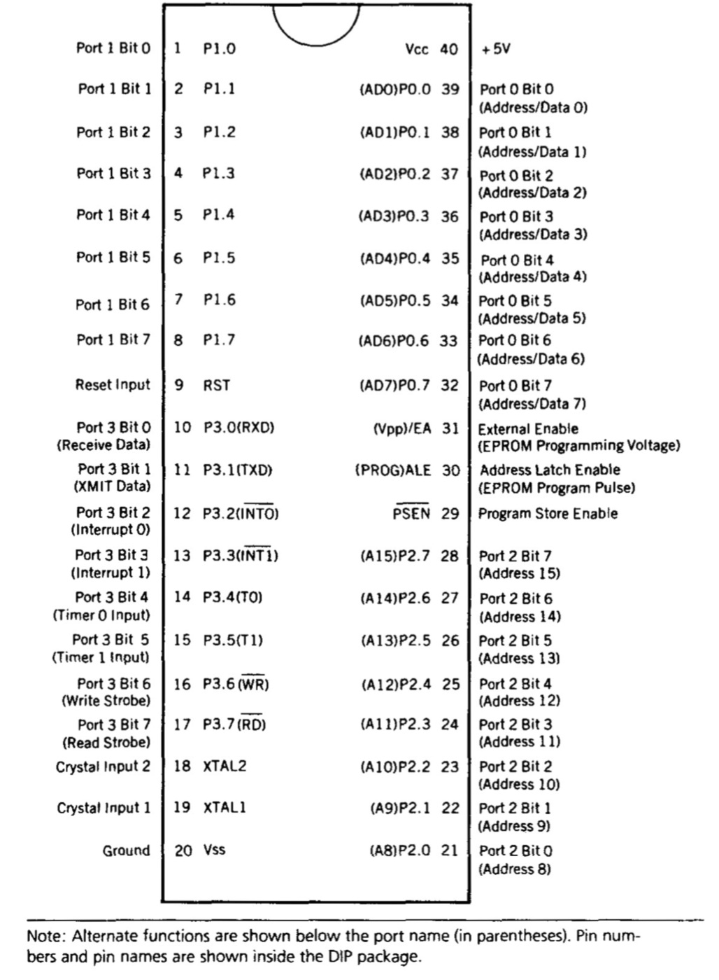
The 8051 microcontroller is packaged in an 40 pin DIP, with the full name and abbreviations for each port on the CPU.
The Oscillator and Clock
All circuits in 8051 are synchronised with the help of a clock. The XTAL1 and XTAL2 pins are provided to connect external oscillators to the chip. The manufacturers decide the maximum and minimum frequencies of the chip.
Program Counter and DPTR
- The Program Counter is an 16 Bit register that points to the memory location holding the current instruction to be executed. The PC can point to a location from
0000hto0FFFhwhen addressing the internal memory, or0htoFFFFh.
- The DPTR register is made up of 2, called DPH and DPT. This is used for memory access for internal and external code.
A and B registers
- 8051 has 34 registers general purpose registers. Two of them are A and B registers are part of the CPU Core.
- The other 32 are arranged in the internal RAM as a part of four banks -
B0-B3of eight registers each -R0 - R7.
- The A accumulator register is the most versatile register available, and is used many operations including arithmetic, logical, and integer multiplication. A is also used for data transfer between any external memory and 8051.
- The B register is used alongside the A register for multiplication and division, and is a general location where data is stored.
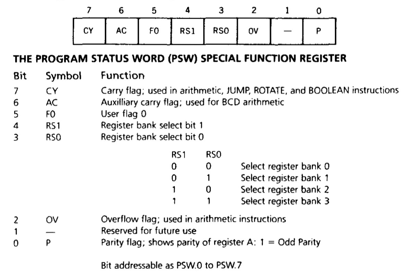
Program Status Word Register
- This register contains a number of flags required for the operation of the CPU. During execution, there is a requirement of flags for recording the outputs of certain instructions and making decisions based on those results. The result of such instructions are stored in 1 bit registers called flags.
- All the flags are conveniently grouped inside the Program Status Word Register, and the Power Control Register, abbreviated as PSW and PCON respectively.
- The PSW register contains four flags that are set during arithmetic operations, two flags that hold the number of the selected register bank, and one general purpose flag that user programs can set.
- One must note that the flags in PSW are user controllable and bit addressable. The math flags are affected by arithmetic operations as well.
- The four math flags held by PSW are Carry(CY), Auxiliary Carry(AC), Overflow(OV) and Parity(P) flags.
Internal Memory
- The 8051 has an Internal RAM and ROM, ROM is where the program instructions are stored, and RAM is where program memory is held. Additional memory can be attached to 8051 through various circuits.
- The 8051 follows the harvard architecture, where a single address can be used to access the RAM and ROM. The circuit automatically selects the appropriate memory based on the nature of the operation.
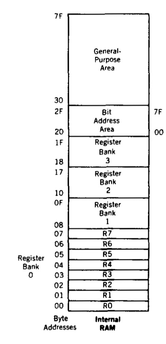
Internal RAM
The 8051 processor come with 128 bytes of in built memory. The memory is segmented as follows:
- The 32 registers are divided in banks of four -
B0 - B3of eight registers eachR0 - R7
- The area from 00h to 1Fh(32 locations) used as general purpose registers.
- The register banks can be accessed through two ways: Either by their memory address, or their number.
- For accessing
R4of theB1bank, I can simply use it’s name provided the bank is selected using the PSW flagsRS1andRS2.
- Or, I can access the
R4ofB1by simply using it’s address0C.
- For accessing
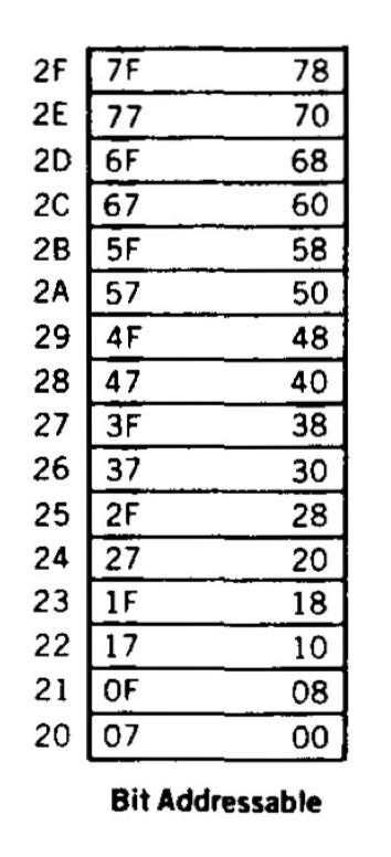
- The area from 20h to 2Fh is called a bit addressable area. Here, each location can either be accessed by bit or a full register can be accessed as a byte.
- For example, if I try to access the location 23h as a byte, it will access the entire register. But, 23h is also the fourth bit of the 24H address.
- The general purpose area is above the bit area, from address 30h to 7Fh and can be accessed as a byte.
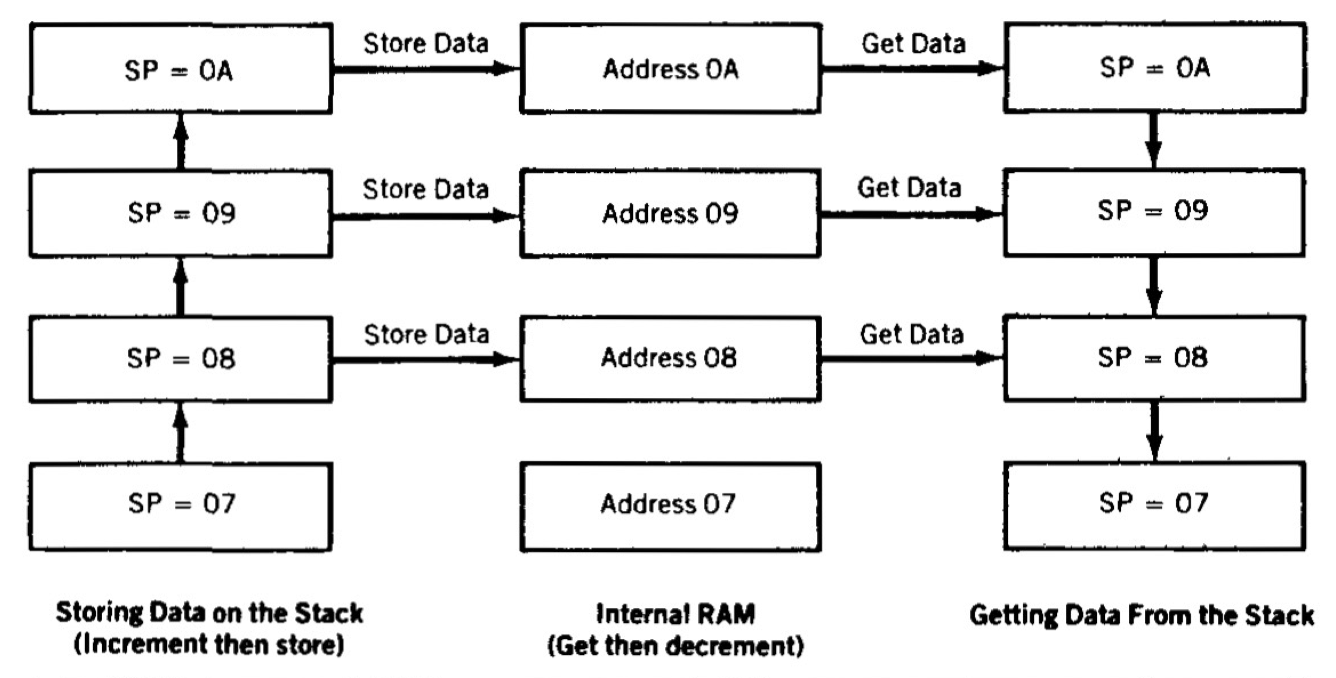
The Stack Pointer
- The stack is a location in the internal RAM used for efficient data storage and retrieval.
- The 8-bit stack pointer (SP) holds the internal RAM address of the topmost data in the stack. When new data is added to the stack, the pointer is incremented. When the stack is read, the pointer is decremented to access the next byte of data. This operation is commonly known as "push" and "pop".
- Upon reset, the SP is set to 07h for the 8051 microcontroller. The programmer can set the stack pointer as needed.
- The size of the stack is limited by the internal RAM. If the stack exceeds its limits, it can overwrite the general-purpose register banks, bit addressable area, and other parts of the RAM. To avoid conflicts with other areas of the internal RAM, it is often placed at a higher address.
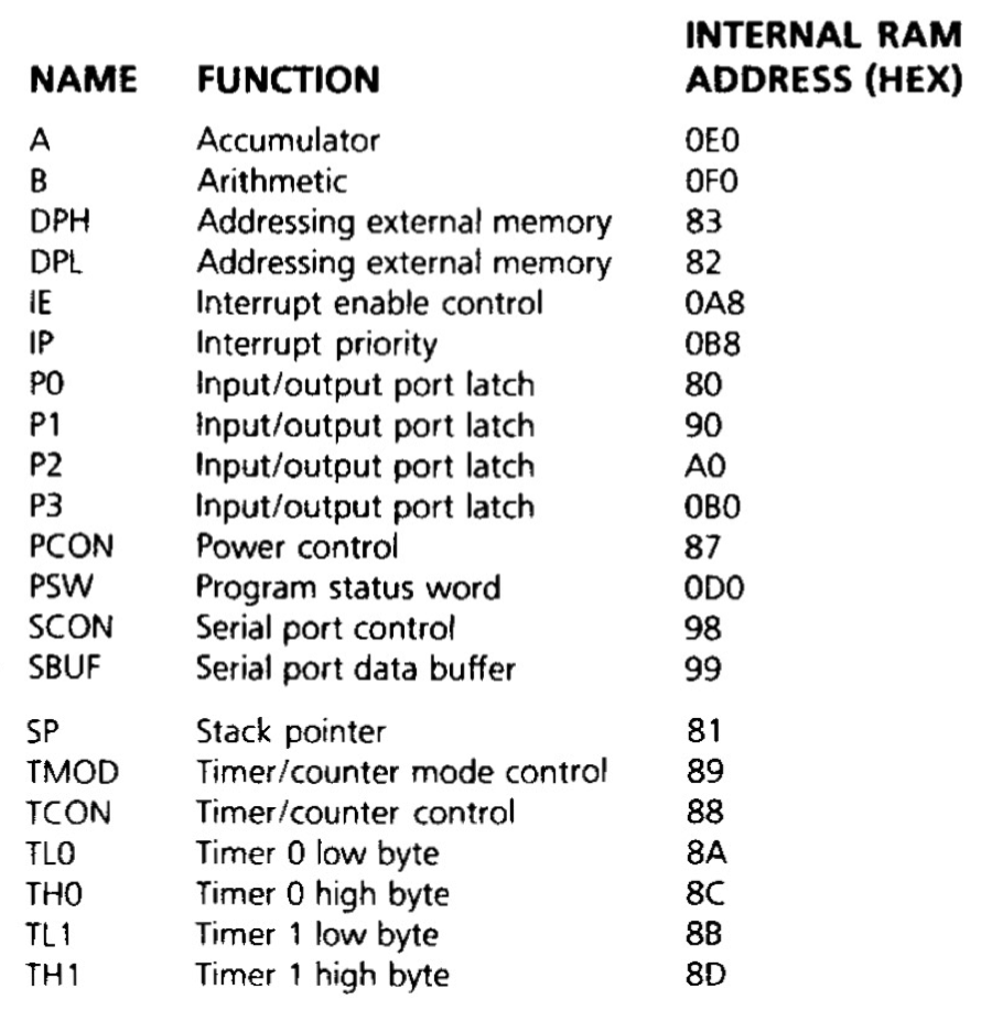
Special Function Registers (SFR)
- Some 8051 internal registers can be accessed by either using their name (only for certain opcodes) or using addresses from 80h to FFh. These registers are often concerned with special instructions, and therefore are called special function registers.
- Some SFR registers are also bit addressable, just like the bit addressable area of internal RAM.
- Not all addresses between 80h to FFh are used for SFRs.
SFRs are named in certain opcodes by their functional names, such asAorTH0, and are referenced by other opcodes by their addresses, such as0E0hor8Ch. Note that any address used in the program must start with a number; thus addressE0hfor the A SFR begins with0. Failure to use this number convention will result in an assembler error when the program is assembled.
Internal ROM
- The 8051 microcontroller allows for separate data memory and program code memory in two different physical memory entities, with the same address ranges.
- The internal program code is stored in an internal ROM from address
0000hto0FFFh.
- The PC (Program Counter) is used to address program code bytes from addresses
0000htoFFFFh.
- When program addresses exceed 0FFFh, which exceeds the capacity of the internal ROM, the 8051 automatically fetches code bytes from external program memory.
- Code bytes can also be exclusively fetched from an external memory at addresses
0000htoFFFFhby connecting the external access pin (EApin 31 on the DIP) to ground.
- The PC is not concerned with the location of the code; it is up to the circuit designer to decide whether the code is stored entirely in internal ROM, entirely in external ROM, or in a combination of both.
Input Output Pins, Ports, and Circuits
From the 40 pins on the DIP, 24 pins can be programmed to be used for one of two entirely different functions, yielding a total of 64 pins in the configuration. The function of a pin totally depends upon what is physically connected to the pin, as well as what the pin is “programmed” to do. Each port has a D-Type output latch for each pin. An 8 bit SFR can be used to control these latches. The eight latches for port 0 are addressed at location 80h; port 0 pin 3 is bit 2 of the P0 - SFR. The data on these latches does not have to the same as the data on the pins. Two data paths allow reading of data from either the latch or the pin. Different opcodes access the latch or the pin accordingly, it depends on how 8051 is connected to external circuitry.
Programmable ports have a control circuitry between the output latch and the port pin. It’s configuration determines the functions of the port pin. Port 1 on 8051 is non programmable, while port 0, 2 and 3 have the control logic. Each pin of port 3 can be individually programmed to be used as either I/O or for alternate functions.
External Memory
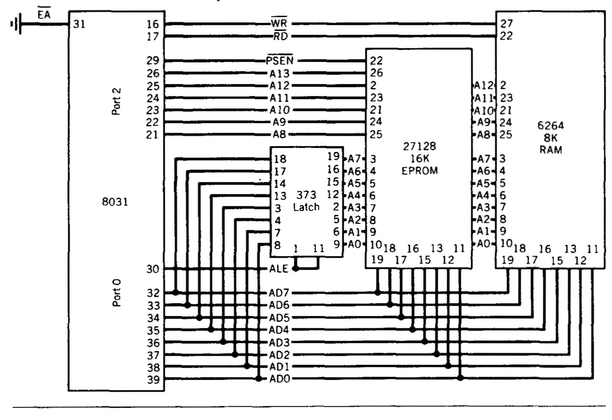
The system designer is not limited to the 4K of ROM and 128 Bytes of RAM internally available in the 8051. The port configurations allow a connection of external EPROMs and RAMs of upto 64K (16 address lines) to the MCU.
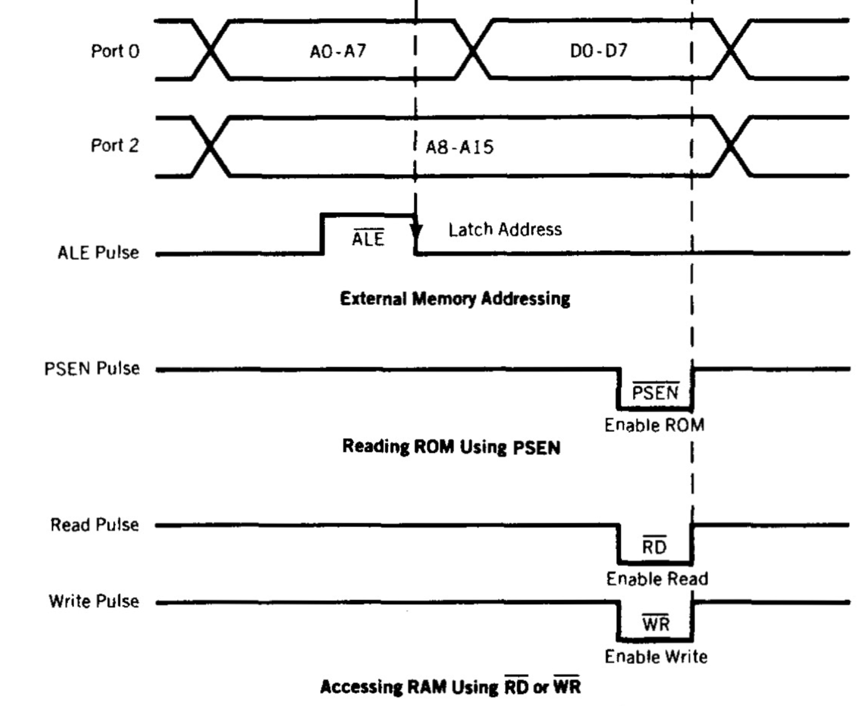
A connection diagram is shown on the right. The 16 bit address lines are divided into two parts, the lower byte connected via a latch. Initially, the address for memory is sent through pins A0-A15, and the latch is enabled once the address has settled on external memory’s pins. This latch is enabled through the ALE pin. This free’s up the A0-A7 pins and allows them to be used as data lines.
When accessing EPROM, we set PSEN` to low once the latch has been set, to allow EPROM to write to the data lines. When trying to read or write to the RAM, the WR` and the RD` pins are set accordingly.
Timers and Counters
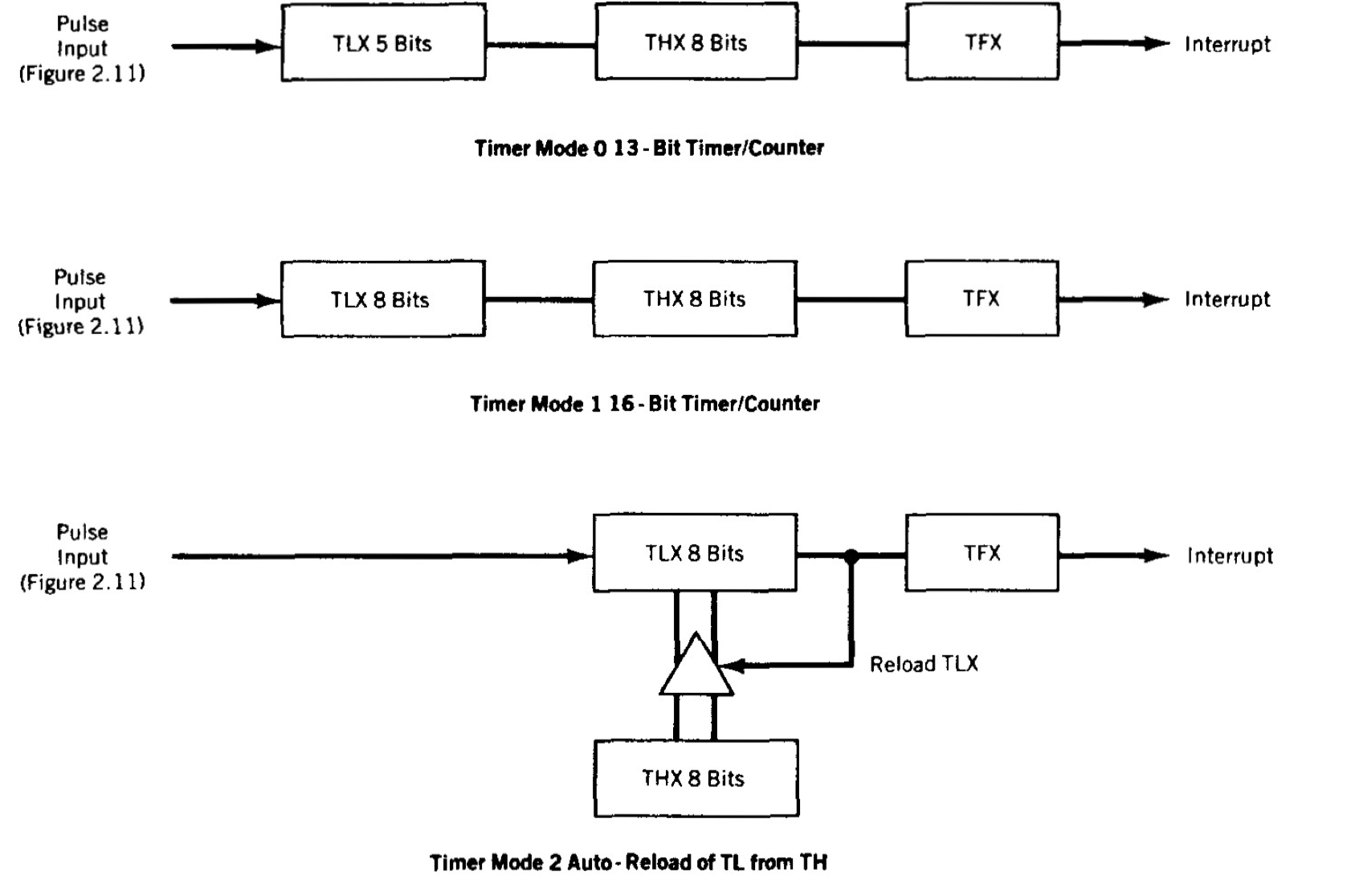
To relieve the processor of the burden of counting, two 16-bit up counters, named T0 and T1, are provided for the general use of the programmer. Each counter may be programmed to count internal clock pulses, acting as a timer, or programmed to count external pulses as a counter.
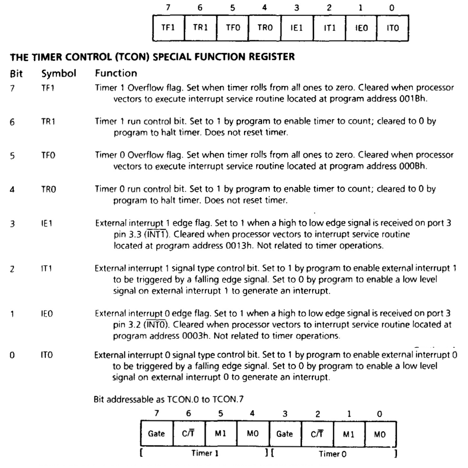
The counters are divided into two 8 bit registers called Timer Low, and Timer High bytes. The counter is controlled using some instructions and bit states in the timer mode control register and timer counter control register, abbreviated as TMOD and TCON respectively. TMOD is solely dedicated to the two timers and is divided into two 4 bit nibbles, each of which control either of the timers. TCON on the other hand has control bits and flags for timers in the upper nibble, and control bits for external interrupts in the lower nibble.
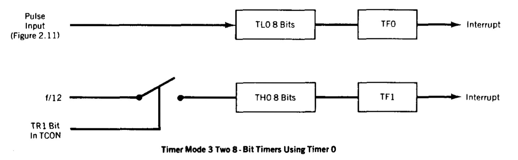
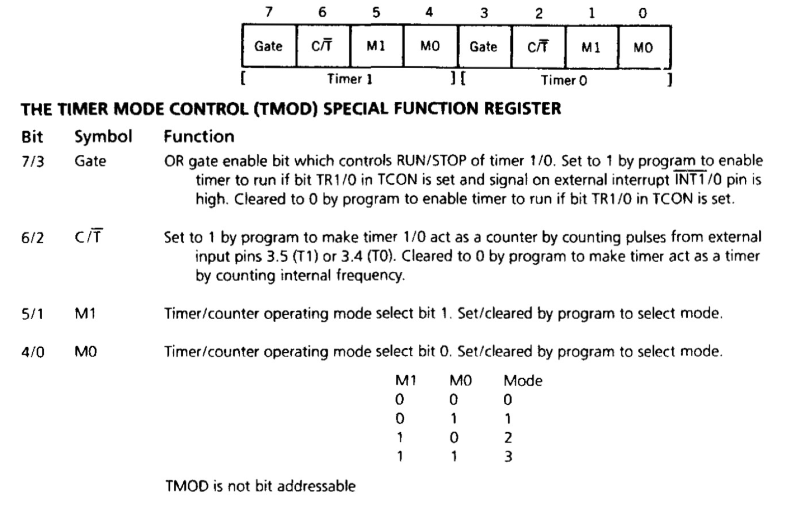
TODO: Write about timer and counter modes
Serial Data Input/Output
The 8051 has a serial data communication circuit that uses register SBUF to hold data. Register SCON controls data communication, register PCON controls data rates. Pins 3.0 (RXD) and 3.1 (TXD) are used for communication.
SBUF physically holds two registers. One is write only and holds data transmitted out of the 8051 via TXD. The other is read only and holds received data from external sources via RXD. Both mutually exclusive registers use address 99h.
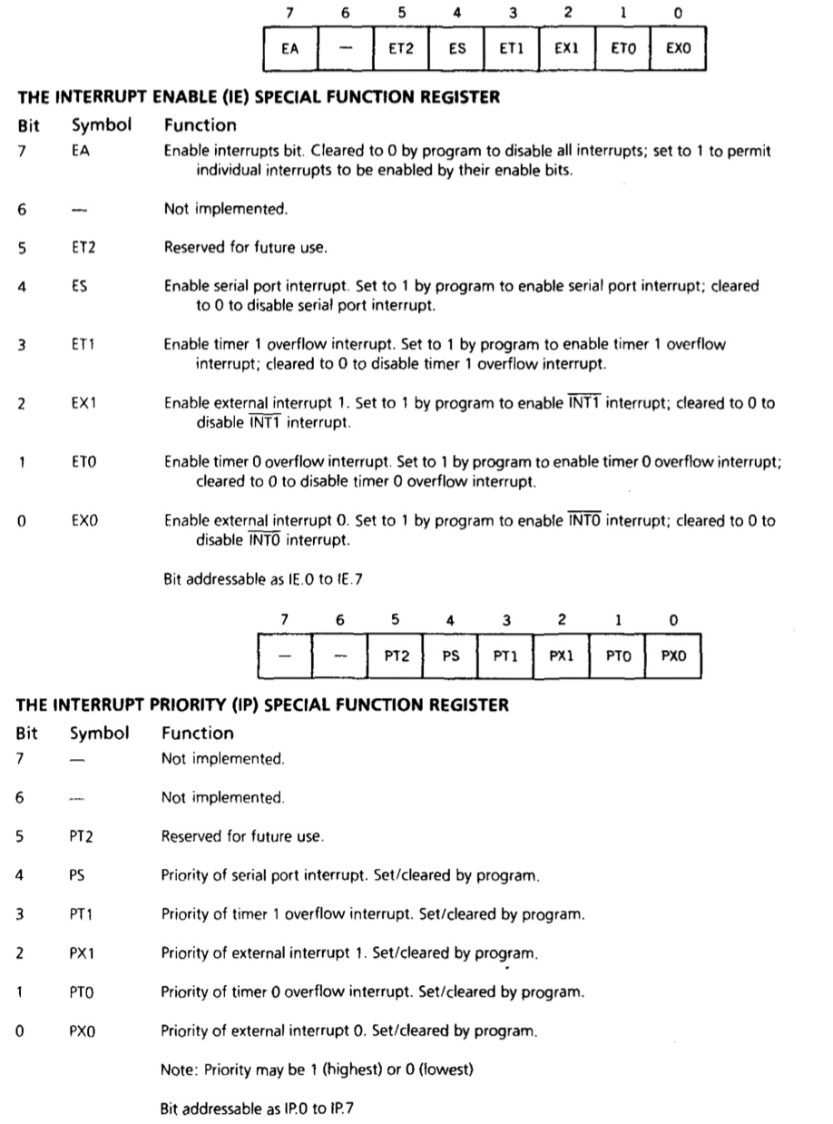
Interrupts
Interrupts may be generated by internal chip operations or provided by external sources. Any interrupt can cause the 8051 to perform a hardware call to an interrupt handling subroutine that is located at a predetermined (by the 8051 designers) absolute address in program memory
- Five interrupts are provided in the 8051.
- If two interrupts with the same priority occur at the same time, then they have the following ranking:
- IE0
- TF0
- IE1
- TF1
- Serial = R1 OR T1
The interrupt saves the PC of the program, which is running at the time the interrupt is serviced on the stack in internal RAM. A call is then done to the appropriate memory location. These locations are shown in the following table:
| IE0 | 0003 |
| TF0 | 000B |
| IE1 | 00013 |
| TF1 | 0001B |
| Serial | 00023 |
A RETI instruction at the end of the routine restores the PC to its place in the interrupted program and resets the interrupt logic so that another interrupt can be serviced.
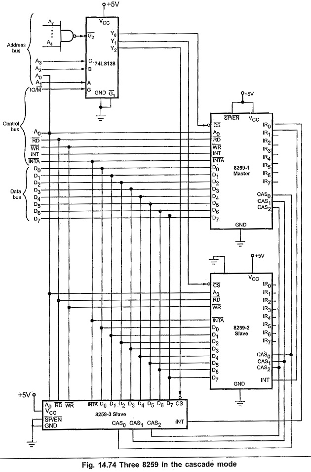
8259 Programmable Interrupt Controller
8259 is a PIC is an IC that is interfaced with various microprocessors for increasing it’s interrupt handling capacity. With a single 8259 IC we can handle 8 interrupts, or we can work with slave 8259s to increase capacity to 64 interrupts.
Components of 8259
In Service Register (ISR)
- It keeps track of which interrupt is in service.
- Eight bit register, each bit indicates which interrupt is in service.
Priority Resolver (PR)
- It examines IRR, ISR and IMR, and determines which interrupt has maximum priority and sends it to the microcontroller.
Interrupt Request Register (IRR)
- It can take eight different interrupts, and the bit of the register is set to one if it receives the corresponding interrupt.
Interrupt Mask Register (IMR)
- It also has eight bits. If any of the bit is set to zero, then the corresponding interrupt is masked.
Control Logic
- It is directly connected to the
INTAandINTpins of Microprocessor.
- It stores the vector addresses during ICW.
Cascade Butter Comparator
- Used to interface with slave/master 8259.
SP/EN- In buffered mode, this pin can be used as an output to control buffer transceivers. In non buffered mode, it is used to designate if master(1) or slave(0).
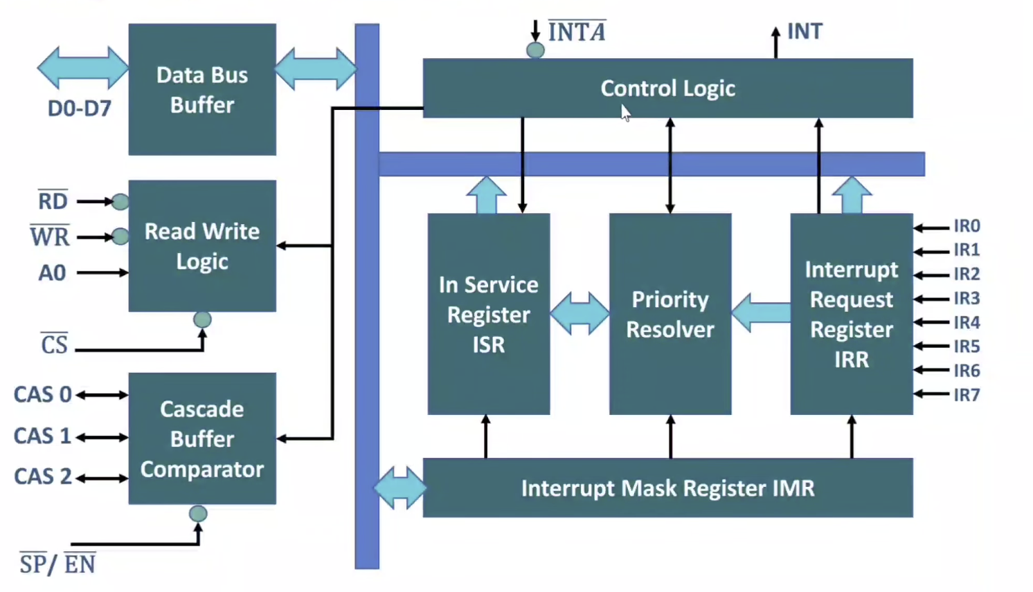
Data Bus buffer
- Used to send Control, Status and Interrupt Vector information to the CPU.
Read Write Logic
- It takes inputs to
RD,WR,A0andCS.
- It holds the Initialisation Command Words(ICW) and Operation Command Words(OCW).
A0pin acts in conjunction withRD,CSandWRpins. It is used to decipher various command words the CPU writes and status that CPU wishes to read.
Flow of interrupts after initialisation
- The IRR receives and stores the Interrupt(s) and marks the corresponding bits as 1 or 0.
- The priority resolver checks against IRR, ISR and IMR and determines which interrupt must be executed by CPU.
- If any interrupt is to be executed, control logic sends
INTto CPU.
- Once CPU receives
INT, it returns anINTA.
- With an
INTA, the ISR sets the bit corresponding to the interrupt as one and the IRR resets the corresponding bit to zero. Alongside, an opcode for CALL instruction is set on the data lines.
- After receiving CALL, CPU sends another
INTAand in response we send lower order byte of CALL address.
- After receiving lower order byte, CPU sends another
INTAand in response we send higher order byte of CALL address.
- After third
INTApulse, ISR is reset and CPU continues to execute subroutine at given vector address.
Programming the 8259 PIC
- 8259 requires two types of command words, the Initialisation Command Word and the Operational Command Word.
- It can be initialised using four ICWs. The first two are essential, and the next two are optional based on the mode of 8259. These words are issued in sequence.
- Once initialised, the 8259 can be set up to operate in various modes by using three different OCWs. However, they no longer need be issued in a specific sequence.
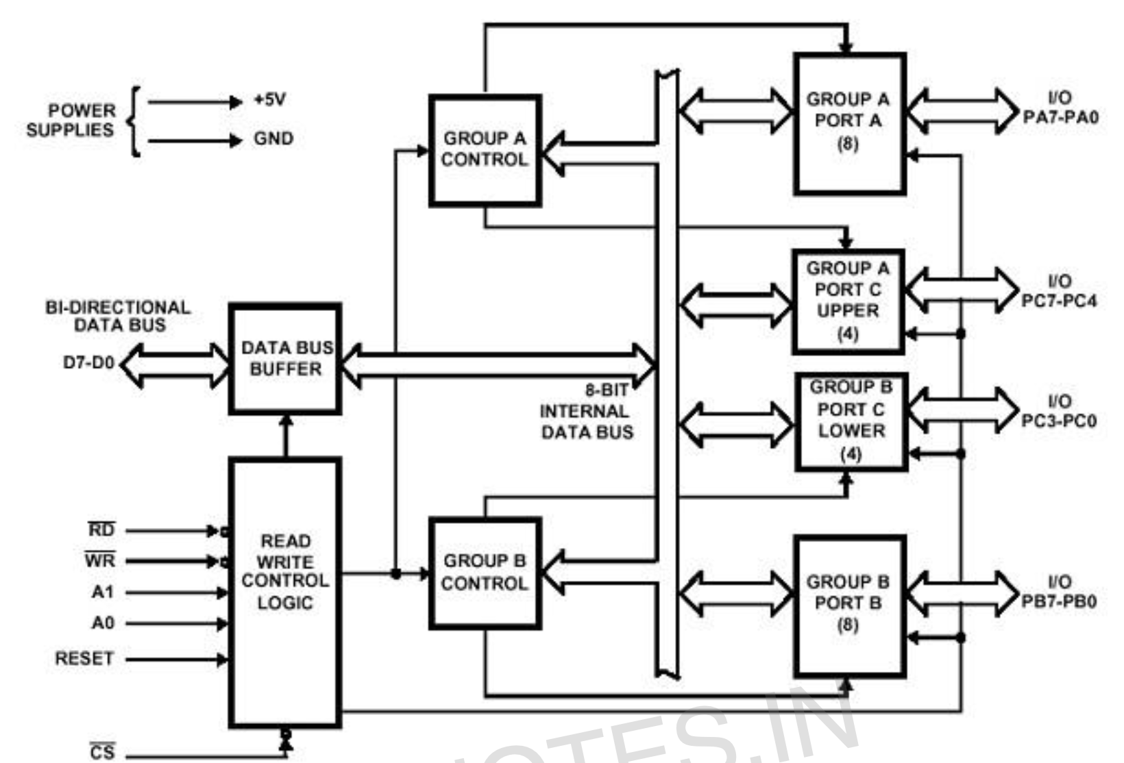
8255 PPI
The 8255 is a general purpose IO device designed to transfer data from I/O to interrupt I/O under certain conditions as required.
Operational Modes
There are two basic operational modes for 8255 IC:
- Bit Set/Reset Mode (BSR)
- Input/Output Mode
These two modes are selected on the basis of the D7 bit provided by the microcontroller. When D7 is 1, 8255 operates in I/O mode, and when D7 = 0, it operates in BSR mode.
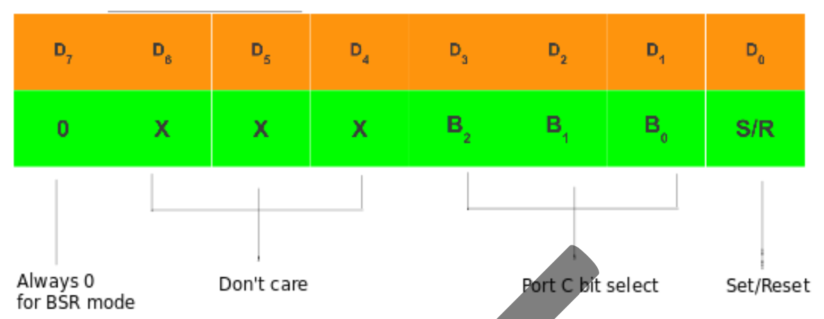
Bit Set Reset Mode
- In this mode, each pin of port C can be set/reset by writing a suitable value to the control word register.
- D7 is always 0 for BSR. D6,5,4 are don’t care bits. D3,2,1 are port C bit select. Finally D0 is used to set/reset the particular pin.
- Eg:
0000 1011will set PC_5 to 1.
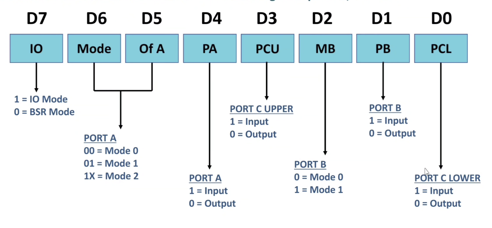
I/O Mode
Mode 0:
- In this mode, basic I/O is done by ports A, B and C. Interrupts are not handled in this mode.
- In this mode, Inputs are buffered and outputs are latched.
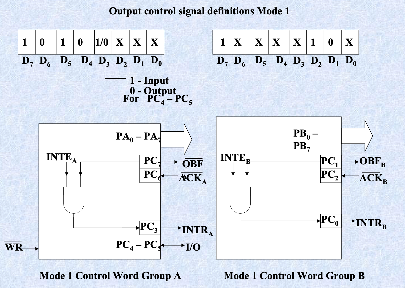
Mode 1:
- In this mode, A and B are used as 8 bit I/O ports, and three bits each from C are used for handshake. Interrupts logic is supported.
- Inputs and outputs are latched.
- The three pins of port C are configured as follows:
- Input:
- (STB) Strobe Input: If this lines falls to logic low level, the data available at 8-bit input port is loaded into input latches.
- Input Buffer Full (IBF): If this lines falls to logic low level, the data available at 8-bit input port is loaded into input latches.
- INTR – This active high output signal can be used to interrupt the CPU whenever an input device requests the service. INTR is set by a high STB pin and a high at IBF pin.
- INTE is an internal flag that can be controlled by the bit set/reset mode of either PC4(INTEA) or PC2(INTEB).
- Output:
- OBF(Output Buffer Full): When this signal becomes low, that means CPU has written data to the specified output port.
- ACK(Acknowledge): This signal is given by an output device, confirms that the data has been transferred from the CPU to the output device.
- INTR – An output signal that can be used to interrupt the CPU when an output device acknowledges the data received from the CPU. INTR is set when ACK, OBF and INTE are 1.
- The INTEA and INTEB flags are controlled by the bit set-reset mode of PC6 and PC2 respectively.
- Input:
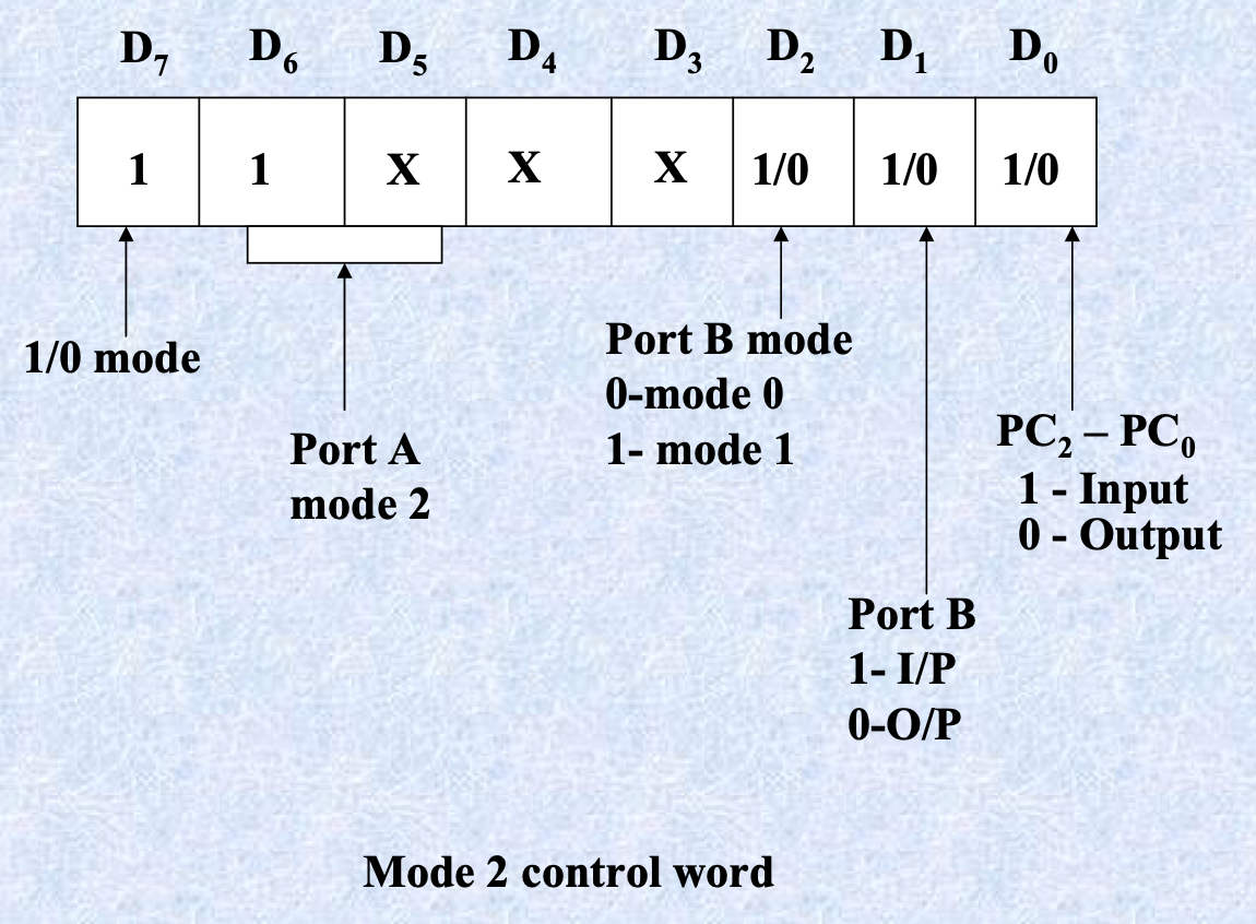
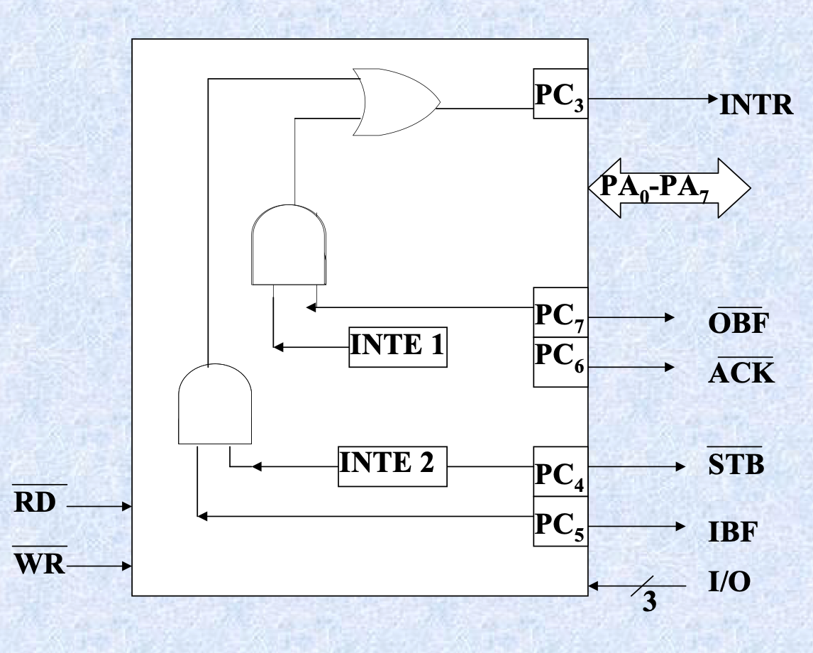
Mode 2:
- In this mode, A is used as a bidirectional mode, and five bits of port C is used for handshake. Interrupt logic is supported. Mode 2 is not available to port B.
- Inputs and outputs are latched.
- The five pins of port C are configured as follows:
- INTR – The CPU is asked for the next data byte to/from it.
- OBF(Output Buffer Full): When this signal becomes low, that means CPU has written data to the output port.
- ACK(Acknowledge): This signal is given by an output device, confirms that the data has been transferred from the CPU to the output device. Now, the data bus can be tri stated and next data byte can be sent to port A.
- (STB) Strobe Input: If this lines falls to logic low level, the data available at 8-bit input port is loaded into input latches.
- Input Buffer Full (IBF): If this lines falls to logic low level, the data available at 8-bit input port is loaded into input latches. This can be used as an acknowledge that the data has been received by the receiver.
- INTR – This active high output signal can be used to interrupt the CPU whenever an input device requests the service. INTR is set by a high STB pin and a high at IBF pin.
- INTE is an internal flag that can be controlled by the bit set/reset mode of either PC4(INTEA) or PC2(INTEB).
- The INTEA and INTEB flags are controlled by the bit set-reset mode of PC6 and PC2 respectively.